Release Date:May 29, 2024 Visit:1689 Source:G-Star Pte.Ltd.
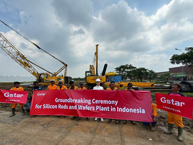
Against the backdrop of continuously rising global demand for renewable energy, solarenergy stands out with its unique advantages. Indonesia, situated near the equator with abundant sunlight resources, has emerged as the largest solar energy market in Southeast Asia, propelled by government support for the photovoltaic (PV) industry. Recently, Gstar held the groundbreaking ceremony for its silicon ingot and wafer factory in Jakarta, Indonesia, signaling the rapid commencement of construction for this modern facility.

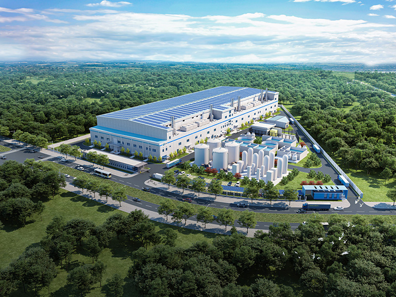
Spanning an area of 60,000 square meters, the factory is strategically located in the Green Industrial Park International Center (GIIC), the largest industrial zone in Indonesia, adjacent to Fortune 500 companies, thus enjoying excellent geographical advantages. With a focus on comprehensive digitization and intelligent manufacturing, the factory has introduced a series of cutting-edge production equipment and technologies,aiming to establish a leading global hub for silicon wafer production.
In its initial phase, the factory will primarily produce monocrystalline silicon ingots and large-size monocrystalline silicon wafers of 182mm and 210mm, which hold extensive application prospects in the solar PV field. Gstar will continually drive technological innovation in the wafer industry, particularly in large-size wafers, thin wafers, and fine-line wafers, to meet the market's demand for higher efficiency and quality PV products.
It's worth mentioning that there are many technical similarities between silicon wafers and semiconductor materials, both heavily reliant on high-purity silicon. Therefore, Gstar's silicon wafer factory not only focuses on the PV industry but also has the potential to extend into the semiconductor wafer production field. In the future, this semiconductor-like factory is expected to undergo technological extensions and industrial upgrades, becoming the first semiconductor wafer production enterprise within the GIIC and expanding Gstar's influence in the semiconductor sector.

The factory is projected to commence production by the end of 2024, achieving an annual capacity of 3 gigawatts (GW) for silicon ingots and3GW forwafers. This capacity expansion will robustly support Gstar's expansion in the global PV module market, meeting the growing market demands. Currently, Gstar's production capacity is in the ramp-up phase and is expected to achieve 3GW of silicon wafers, 3GW of battery wafers, 12GW of frames, and 3GW of module production capacity by the end of 2024, completing the integrated layout of ingot pulling, silicon wafer, battery wafer, frame, and module. By then, Gstar's comprehensive strength and risk resistance will be further enhanced.
Gstar adheres to a strategic layout of industrial vertical integration, committed to independent research, design, production, and sales from silicon wafers and battery wafers to frames and modules. This vertical integration model not only helps ensure product quality but also ensures the stability of the supply chain, while bringing about price advantages and production efficiency improvements. The commencement of the silicon wafer factory construction is a significant step taken by Gstar under this strategic guidance.
Looking ahead, Gstar will continue to actively guide close cooperation along the upstream and downstream industrial chains, accelerating its layout and development in the PV field. We firmly believe that under such leadership, the global PV industry can achieve faster and healthier development. Let us look forward to the rise of this modern factory together and anticipate Gstar's creation of a brighter future in the PV field.